

This page explains the design and construction of special printed circuits for student use in teaching and assessing troubleshooting skills.
The basic idea is the design of portable, rugged, and inexpensive printed circuits allowing for instructor-placed component faults which the student must properly identify using only electronic test equipment (and not by visual inspection!). Each PCB has a set of test points on the top side for students to connect multimeter or oscilloscope leads, and 3-pin headers with connecting ``jumpers'' on the bottom side providing a convenient way for the instructor to place hidden, shorted and/or open faults for individual components. The PCB attaches to the top of a plastic box which serves to hide the fault jumpers on the bottom side, allowing students access only to the top side with the components and test points.
These PCBs have proven invaluable to me in the instruction of my students. I use them regularly as hands-on performance assessments in the courses I teach. The boards are so convenient to use, in fact, that I even incorporate them into tests given in a regular classroom, not a lab room!
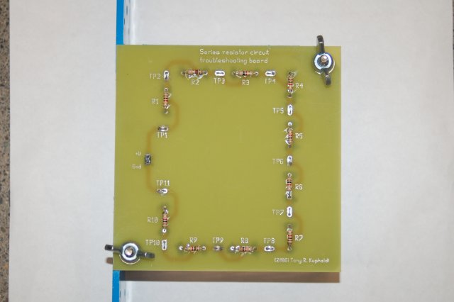
The simplest troubleshooting circuit I've made for students to use is a 10-resistor series circuit, shown here (click to enlarge):
Underneath this board lurks a nine-volt battery to power the circuit. Since the battery (and the fault jumpers) are safely tucked inside the blue plastic box while the student is diagnosing the circuit, the circuit is constantly powered during the exercise which prevents students from simply using an ohmmeter to look for shorts or opens. With the circuit constantly powered, the student can only take voltage measurements, which is a better test of electronic troubleshooting ability. The battery may be seen in the following photo (click to enlarge):
A view of the circuit board's bottom side reveals the fault jumpers, used to ``program'' either open or short faults for each resistor in the circuit. The battery unplugs, so as not to discharge it while the PCB is being stored (click to enlarge):
The following close-up shot shows how the fault jumpers work. All jumpers in this photograph are in their ``normal'' positions, where the respective components function as they should. Moving any jumper to the adjacent position (connecting the middle header pin to the other header pin) shorts out the component. Removing the jumper completely (or moving it so it fits on only one header pin) opens the component (click to enlarge):
The plastic box used to cover the bottom side of the PCB is nothing more than a standard 4x4 inch electrical junction box used for home wiring. It costs less than 2 dollars where I live, and may be easily equipped with 8-32 machine screws and wingnuts to securely attach the PCB. Two holes in the PCB are precisely spaced to match the two screws on the box (click to enlarge):
This close-up shows how an 8-32 screw is threaded tightly into one of the two existing plastic holes in the box. Thus, the box itself need not be altered:
Another troubleshooting PCB is show here -- a loaded voltage divider circuit (click to enlarge):
Another troubleshooting PCB is show here -- a quarter-active Wheatstone bridge circuit with temperature sensor (click to enlarge):
The following schematic diagrams show the design of the fault jumpers, both for simple short and open faults, and also for more sophisticated partial-short and partial-open faults:
In case you were wondering, the ``plain'' look of my printed circuit boards is the result of me opting to go with the cheapest board manufacture I could find: a ``bare-bones'' PCB option where there is no soldermask or silkscreen added to the boards -- only tinned copper. This results in a cost of about $17 for each PCB, plus the cost of the componentry. This price is quite favorable to the cost of comparable PCB-based troubleshooting tools on the market, and the layout is simple enough for a novice PCB artist (such as myself) to handle with ease.
Like all other materials on this site, these printed circuit board designs and schematics are licensed under the Creative Commons Attribution-only license, giving you freedom to copy and/or improve my ideas for use in your own courses.